Design Tips
To avoid delay please submit following information with your order:
Gerber Files that can go straight to production avoiding costly delays.
We can use Gerber files in either 274D or 274X format for all layers, including silkscreens and soldermasks.
If using 274D format, we require a separate aperture list/report File, this will tell us the pad and line sizes you used to design the board.
Tool file/chart, telling us which tool is what size and how many of each tool is used
Fabrication drawing or Manufacturing Requirements.
NC Drill file in ASCII format.
Example:
%
T01
X045Y0075
X03525Y01225
M30
Readme file. It is a good idea to include a readme file with information such as; contact person’ name, phone/fax number and other information about your board requirements, this would aid in quickly moving your job from pre-engineering to production floor. This file can be in either ASCII (*.TXT) or Microsoft Word (*.DOC) format
Note: We also can support CAD files, such as Protel series, PADS2007, AutoCAD.But we have to output Gerber Files before CAM process.
Design Tips
Hole Size and Pad Size:
For power and ground layers, make the clearance 26mil larger than the hole size. For component, solder and inner layers make the pad size 16mil larger than the hole size. It allows more room for drilling and decreases the chances for shorts. Soldermask pads should be 5mil larger than the soldering pad.
Draws and Flashes:
When designing a board, try to limit the amount of draws you use. Draws use a lot of memory and slows the programming time. Ex.: Use a flash for pads instead of draws. If for some reason we need to increase or decrease that pad size, it can easily be done by changing the D-code, if they are done with draws it could be a nightmare.
Silkscreen rules:
Keep silkscreen at least 6mil away from pads (except vias). The minimum line width is 4mil and the minimum letter height is 28mil. Ensure that no silkscreen falls on any pads this could affect the soldering process. Avoid printing component outlines, especially if you are using automatic assembly.
Routing:
To speed programming - add a borderline to one of your files, this will give us a route reference for routing the PCB to size. On the other hand keep routing at least 15mil away from copper except the edge will be exposed copper or plated.
Cost Cutting Tips:
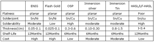
Surface treatment:
All surface treatment methods have their advantages and disadvantages; the decisive factor is, of course, their application. A short overview of the most common surface treatments is given below.
|